


What Is a PCB? Complete Guide to PCB Manufacturing, Assembly & Working Principle
What Is a PCB and How Does It Work?
A printed circuit board (PCB) is a flat, rigid or flexible substrate that mechanically supports and electrically connects electronic components using conductive copper traces, pads, and vias etched or deposited onto and through layers of insulating material. Every electronic device — from a smartphone to an industrial controller to a medical instrument — operates because its components are interconnected by a PCB.
How a PCB works can be understood in three layers: the physical substrate provides mechanical support and electrical isolation; the copper layer pattern routes electrical signals and power between connection points; and the components mounted on the board perform the actual electronic functions — amplifying signals, switching current, storing data, processing instructions, or filtering noise.
The base material of most PCBs is FR-4 fiberglass epoxy laminate — a woven glass fabric impregnated with epoxy resin, pressed into rigid sheets, and clad with copper foil on one or both sides. FR-4 offers a practical combination of mechanical strength, electrical insulation, flame resistance, and dimensional stability that suits the majority of commercial and industrial applications. Specialty substrates include Rogers high-frequency laminates for RF and microwave boards, polyimide (Kapton) for flexible circuits, and aluminum-core or copper-core metal-backed boards for high-power LED and power electronics applications.
PCBs are classified by their layer count and construction:
- Single-layer PCB — copper traces on one side only; used in simple, low-cost products such as power supplies, LED drivers, and basic consumer electronics
- Double-layer PCB — copper on both sides, connected by plated through-holes; the most widely produced type, covering the majority of industrial, automotive, and consumer electronics applications
- Multilayer PCB — 4, 6, 8, or more copper layers laminated together with insulating prepreg material; used in high-density designs where component count, signal integrity, and EMI shielding requirements exceed what two-layer routing can achieve; smartphones, servers, and aerospace electronics typically use 8–16 layer boards
- HDI (High Density Interconnect) PCB — multilayer boards with microvias (laser-drilled holes as small as 75 µm diameter), fine-pitch traces (under 100 µm), and buried or blind vias; enables the extreme component density required in mobile devices, wearables, and advanced packaging applications
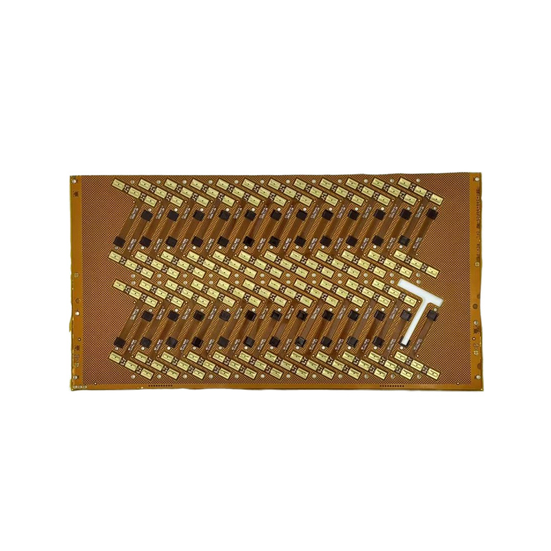
- Flexible and rigid-flex PCB — polyimide-based circuits that bend or fold into three-dimensional configurations; used in cameras, medical implants, aerospace sensors, and any application where the circuit must conform to a non-planar mechanical envelope
PCB Manufacturing Process: How a PCB Is Made
PCB manufacturing — also called PCB fabrication or PCB fab — is the process of producing the bare board before any components are mounted. It begins with design files and ends with a tested, bare copper-patterned substrate ready for assembly. The full manufacturing process of a PCB for a standard double-sided FR-4 board follows this sequence:
- Design file generation and DFM review — the PCB designer outputs Gerber files (or ODB++ format) describing each copper layer, solder mask, silkscreen, drill locations, and board outline. The fabricator reviews these files against design-for-manufacturing rules: minimum trace width and spacing, annular ring size, aspect ratio of drilled holes, and panel utilization efficiency.
- Inner layer imaging (multilayer boards) — copper-clad laminate panels are coated with a photosensitive dry film resist, exposed to UV light through a photoplotted film or direct laser imaging tool, and developed to reveal the circuit pattern. The exposed copper is then etched away in a chemical bath (typically cupric chloride or ammoniacal etchant), leaving only the desired trace pattern. The resist is then stripped.
- Lamination (multilayer boards) — inner copper layers are inspected by automated optical inspection (AOI), then stacked in sequence with prepreg (partially cured glass-epoxy) sheets between them and outer copper foil on top and bottom. The stack is pressed in a heated hydraulic press at 175–200°C and 200–400 psi for 60–120 minutes, fusing all layers into a single rigid panel.
- Drilling — CNC drilling machines equipped with carbide twist drills create through-holes for vias and component leads. Modern high-density boards use laser drilling (CO₂ or UV-YAG lasers) for microvias smaller than 150 µm. Drill registration accuracy is critical — positional tolerance for production drilling is typically ±75 µm or better.
- Electroless copper deposition (PTH — plated through-hole) — a thin layer (1–3 µm) of copper is chemically deposited onto all drilled hole walls and bare laminate surfaces. This conductive seed layer enables the subsequent electroplating step to build up the copper in the holes to the specified plating thickness, typically 25 µm minimum in the barrel for IPC Class 2 boards.
- Outer layer imaging and plating — the outer copper surfaces are coated with dry film resist, imaged, and developed as with the inner layers. Copper is electroplated into the exposed traces and hole walls. Tin or tin-lead plating is then applied as an etch resist. After stripping the dry film, the unwanted base copper is etched away, and the tin etch resist is stripped, leaving the final copper pattern on the outer layers.
- Solder mask application — a liquid photoimageable (LPI) solder mask is screen-printed or curtain-coated over the entire panel surface, then exposed and developed to open windows over pads while covering all traces. Solder mask provides electrical isolation, protects copper from oxidation, and prevents solder bridging between adjacent pads during assembly. The most common color is green, though black, blue, red, and white are standard options.
- Surface finish application — exposed copper pads receive a surface finish to prevent oxidation and ensure solderability. The major finish options are: HASL (hot air solder leveling — most economical, not suitable for fine-pitch SMD), ENIG (electroless nickel immersion gold — flat, reliable, widely used for fine-pitch and BGA pads), OSP (organic solderability preservative — low cost, fine-pitch compatible, single reflow window), ENEPIG (electroless nickel, electroless palladium, immersion gold — premium finish for wire bonding and mixed technology), and immersion silver or immersion tin.
- Silkscreen (legend) printing — reference designators, component outlines, polarity marks, logos, and revision identifiers are inkjet-printed or screen-printed onto the board surface over the cured solder mask.
- Electrical test — the bare board is tested on a flying probe machine or a dedicated bed-of-nails fixture that verifies continuity of all nets and absence of shorts between isolated nets. IPC-9252 governs the electrical test requirements for bare boards.
- Routing, scoring, and V-grooving — individual boards are routed from the production panel using CNC routing machines or V-scored (a V-shaped groove cut partially through the panel on both sides) for breakout after assembly. Tab-routing with mousebites is standard for irregular board shapes.
What Is PCB Assembly (PCBA)?
PCB assembly (PCBA) is the process of populating a bare PCB with electronic components and soldering them in place to create a functional circuit board. The distinction between PCB manufacturing and PCB assembly is fundamental: fabrication produces the board; assembly places and connects the components. A PCBA (printed circuit board assembly) is the completed unit — board plus components plus solder joints — ready for integration into a product or for final testing.
Modern PCB assembly encompasses three primary component attachment technologies, which are frequently combined on the same board:
- SMT (Surface Mount Technology) — components with no leads or very short gull-wing/J-bend leads are soldered directly onto pads on the board surface. SMT enables very high component density and is processed entirely by automated machines. Over 90% of components in modern electronics are SMT types.
- THT (Through-Hole Technology) — components with wire leads that pass through drilled holes and are soldered on the opposite side. THT provides stronger mechanical attachment than SMT and is retained for connectors, large capacitors, transformers, and components subject to mechanical stress.
- Mixed technology — the majority of real-world boards combine SMT and THT components, processed in a defined sequence: SMT side one → reflow → flip → SMT side two → reflow → THT insertion → wave or selective solder.
PCB Assembly Process Steps: The Complete Sequence
The PCB assembly process follows a well-defined sequence. Each step is governed by process parameters — stencil thickness, paste viscosity, reflow profile, wave solder temperature — that must be controlled within specification to achieve consistent, reliable solder joints at volume production rates.
- Solder paste printing — a stainless steel or nickel stencil with laser-cut apertures corresponding to each SMT pad is aligned over the bare PCB in a screen printer. A squeegee blade forces solder paste (a suspension of tin-silver-copper or tin-lead alloy powder in flux vehicle) through the apertures onto the pads. Stencil thickness (typically 100–150 µm) and aperture dimensions control the volume of paste deposited. Consistent paste volume is the single largest predictor of downstream solder joint quality.
- Solder paste inspection (SPI) — a 3D SPI machine measures paste volume, height, area coverage, and X-Y offset for every pad on the board immediately after printing. Boards with paste defects — bridging, insufficient volume, or misregistration — are rejected or reworked before components are placed. SPI before placement prevents the much more expensive defect of tombstoned or open-jointed components discovered after reflow.
- SMT component placement (pick and place) — automated pick-and-place machines remove SMT components from tape-and-reel, tray, or tube feeders using vacuum nozzles and place them onto the solder paste deposits at high speed. Modern high-speed chip shooters achieve placement rates of 50,000–100,000 components per hour for small passives; precision placement heads for fine-pitch ICs, BGAs, and QFNs operate at lower speeds with vision-guided alignment systems achieving ±25 µm placement accuracy.
- Reflow soldering — the populated board travels through a multi-zone reflow oven on a conveyor. The oven's temperature profile — preheat ramp, soak zone, reflow peak, and cooling rate — is programmed to activate the flux, melt the solder alloy (peak temperature 235–250°C for SAC305 lead-free, or 210–220°C for Sn63Pb37 leaded), wet the component terminations and PCB pads, and then solidify into reliable metallurgical joints. Nitrogen atmosphere reflow is used for oxidation-sensitive components and fine-pitch assemblies.
- Automated optical inspection (AOI) — 2D or 3D AOI systems image every component and solder joint on the reflowed board using structured light, multiple cameras, or laser triangulation. AOI verifies component presence, polarity, value (by color band or marking), and solder joint shape. Defect coverage for well-programmed AOI systems typically exceeds 95% for visible defects; hidden joints under BGAs and QFNs require X-ray inspection.
- Through-hole component insertion — for boards with THT components, axial and radial leads are inserted manually or by robotic insertion machines after the SMT reflow process. Connectors, large electrolytic capacitors, and transformers are the most common THT components in mixed-technology assemblies.
- Wave soldering or selective soldering — THT boards pass over a molten solder wave (typically at 250–265°C) that contacts the bottom side of the board, wetting through-hole barrels and forming fillets on both component and board sides. Selective soldering machines use a miniature nozzle or fountain to solder specific through-hole areas on boards where the bottom side carries SMT components that cannot be exposed to the full wave.
- Cleaning — flux residues from both reflow and wave solder processes are removed by inline or batch aqueous wash systems, semi-aqueous cleaning, or vapor degreasing, depending on the flux type used. No-clean flux assemblies may skip this step, but cleaning is mandatory for medical, aerospace, and high-reliability industrial assemblies.
- Manual assembly and rework — components that cannot be placed by machine — hand-wound transformers, battery holders, wire harness connectors, press-fit pins, and certain large heat sinks — are installed manually. Partial manual assembly within an otherwise automated line is standard for products with mixed component types. Rework of identified defects is performed using hot air rework stations, soldering irons, and BGA reballing equipment.
- Conformal coating (where specified) — a protective polymer coating — acrylic, silicone, polyurethane, or epoxy — is spray-applied, selectively dispensed, or dip-coated over the completed PCBA to protect against moisture, dust, chemical corrosion, and condensation. Required for automotive, outdoor, marine, and industrial electronics operating in harsh environments.
- Functional test and ICT — in-circuit test (ICT) uses a bed-of-nails fixture to probe test points across the board and verify component values, continuity, and absence of shorts. Functional test applies power and input signals to verify that the assembled board performs its intended electronic functions within specification. Both test stages generate data used for process control and traceability.
PCB Pick and Place: The Core of SMT Assembly Automation
PCB pick and place machines are the central equipment in any SMT assembly line. They account for the majority of the assembly line capital cost and directly determine the speed, accuracy, and flexibility of the production operation. Understanding how pick and place machines work and how they are specified helps engineers and procurement teams match equipment capability to product requirements.
Pick and place machines operate using one or more placement heads mounted on an X-Y gantry or rotating turret structure. Each head carries a vacuum nozzle sized to the component being picked. The machine's vision system — typically a bottom-illuminated upward-looking camera — captures the component after pickup to measure its actual position and angle relative to the nozzle center, and compensates for pickup offset before placing the component on the paste-printed board.
Machine categories reflect the tradeoff between speed and placement accuracy:
- High-speed chip shooters — rotating multi-nozzle turret heads placing 0402, 0201, and 01005 passive components at 50,000–120,000 CPH (components per hour); placement accuracy ±50–75 µm at 3σ
- Flexible placement machines — multiple independently controlled heads handling components from 01005 up to 50×50 mm; 10,000–30,000 CPH; accuracy ±25–50 µm at 3σ; the workhorse machine for mixed-component boards
- High-accuracy precision placers — dedicated machines for fine-pitch CSPs, flip chips, and optical components; 1,000–5,000 CPH; accuracy ±10–15 µm at 3σ with active alignment
Component feeders — tape-and-reel feeders for SMD components on 8, 12, 16, or 24 mm carrier tape; matrix trays for IC packages; and stick or tube feeders for DIP and connector-style components — determine the machine's component variety capacity. A well-configured pick-and-place line for a complex PCBA may run 100–200 feeder positions simultaneously, with automatic feeder-change alerts triggered by low-part counters.
PCB Design and Assembly: How Design Decisions Affect Manufacturability
PCB design and assembly are deeply interdependent. Design decisions made in EDA software — pad dimensions, component spacing, via placement, panel fiducial locations, test point accessibility — directly determine whether the board can be assembled at yield and cost targets, or whether it will generate chronic defects and rework on the production line.
The most impactful design-for-assembly (DFA) principles that every PCB designer should apply:
- Component orientation consistency — aligning all polarized components (capacitors, diodes, ICs) in the same direction significantly reduces placement programming time and human error risk. All component pin 1 indicators in one corner direction is the most assembly-friendly layout convention.
- Adequate courtyard clearance — IPC-7351 land pattern standards define component courtyard boundaries. Violating courtyard clearance between adjacent components prevents the pick-and-place nozzle from clearing neighboring components and forces manual placement or assembly sequence workarounds.
- Fiducial marks — a minimum of three global fiducials (1 mm copper circles in clear solder mask openings) in three corners of the panel and local fiducials adjacent to fine-pitch ICs and BGAs are required for accurate machine vision registration. Missing fiducials are one of the most common fabrication-to-assembly interface failures.
- Via-in-pad avoidance — placing vias inside SMT pads causes solder to wick down the via barrel during reflow, starving the joint of solder and creating open or weak connections. Where via-in-pad is unavoidable for routing density, the via must be filled and capped during PCB fabrication before assembly.
- Test point placement — locating accessible, 1 mm minimum diameter test pads for every net on a dedicated test point grid enables efficient ICT fixturing and dramatically reduces functional test coverage gaps.
PCB Prototype and Assembly: From Design Files to First Build
PCB prototype and assembly services bridge the gap between completed design and validated, producible product. Prototype builds serve a different set of priorities than volume production: the emphasis is on speed-to-first-article, flexibility to handle engineering changes, and access to process data that informs design revisions.
The PCB prototype process typically follows this timeline for a standard 4-layer FR-4 board:
- PCB fabrication — 24–72 hours for expedited prototype fabrication; standard lead time is 5–10 working days. Most prototype fabricators offer online DFM checks and instant quoting based on Gerber file uploads.
- Component procurement — the critical path for most prototypes. Long-lead-time ICs (FPGAs, specialized ASICs, power management ICs) may require 8–16 weeks from distribution stock or factory order. Prototype builds often use existing engineering inventory or accept substitutions on non-critical passives to accelerate the build schedule.
- Assembly — prototype assembly runs (typically 1–20 boards) are processed on the same SMT lines as production, but without the full jig and fixture investment. Stencil printing is performed with a framed stencil or frameless foil tensioned in a universal holder; pick-and-place programming is performed from the centroid/XY coordinate file and BOM provided with the Gerber package.
- Partial manual assembly — prototype quantities often include components not yet on feeder tape (loose parts in cut strips, bag-and-label quantities, or engineering samples), requiring hand placement. Experienced prototype assemblers can hand-place 0402 and even 0201 components under microscope, and hand-solder fine-pitch QFP and QFN packages — capabilities that distinguish a capable prototype house from a pure volume production facility.
PCBA manufacturing at prototype stage also commonly involves non-standard elements: battery connectors, display interface FFC/FPC connectors, housing snap-fit standoffs, and RF coaxial connectors — all typically hand-assembled. The combination of automated SMT and partial manual assembly for specialized connectors, screens, batteries, and housings is the standard mode for prototype and low-volume production builds, and most contract manufacturers structure their prototype services to accommodate this mixed workflow without premium surcharges.
PCB Assembly and Soldering: Reflow, Wave, and Selective Methods Compared
Soldering is the core joining process in PCB assembly, and the method selected for each joint type has major implications for joint quality, thermal stress on components, and process yield. The three principal PCB assembly and soldering methods each address different component types and board configurations.
| Method | Component Type | Peak Temperature | Throughput | Key Limitation |
|---|---|---|---|---|
| Reflow soldering | SMT (all types) | 235–250°C (lead-free) | Very high | Requires paste printing and pick-and-place upstream |
| Wave soldering | THT, bottom-side SMT | 250–265°C | High | Cannot solder top-side SMT; shadowing behind tall components |
| Selective soldering | THT on mixed boards | 260–270°C at nozzle | Medium | Lower throughput than wave; nozzle wear for high-density areas |
| Hand soldering | Rework, connectors, wires | Variable (tip 300–380°C) | Low | Operator-dependent quality; thermal stress risk on adjacent SMT |
The soldering method also determines the alloy specification. SAC305 (96.5% tin, 3% silver, 0.5% copper) is the dominant lead-free alloy for reflow and wave applications in commercial electronics — it offers a melting point of 217°C, good mechanical properties, and compatibility with most PCB surface finishes. Sn63Pb37 eutectic solder (183°C melting point) remains in use for military, aerospace, and legacy medical electronics under RoHS exemptions, where its superior thermal fatigue resistance and lower processing temperature are valued over environmental compliance concerns.
How to Use a PCB Board: Integration, Testing, and Handling Guidelines
Once a PCBA is delivered, correct handling, integration, and initial power-up procedures determine whether it performs as designed from the first use. The following guidelines apply to engineers, technicians, and product developers working with assembled PCBs.
- ESD precautions — always handle PCBAs at a grounded ESD workstation wearing a wrist strap. CMOS logic, MOSFETs, and RF components can be permanently damaged by electrostatic discharge events below 100 V — well below the threshold of human perception. Store boards in antistatic bags or conductive foam when not in use.
- Visual inspection before power-up — verify there are no visible solder bridges between adjacent pads, no missing components, no cracked or lifted pads, and no visible foreign material (solder balls, wire clippings) on the board surface. A 10× loupe or digital microscope is adequate for initial inspection.
- Initial power-up procedure — apply power through a current-limited bench supply set slightly above the board's expected idle current draw. A sharp current spike during power-up — especially one that triggers the current limit — indicates a solder bridge or shorted component that must be located and corrected before normal operation.
- Connector mating forces — do not force connectors. FFC/FPC ribbon connectors, board-to-board connectors, and fine-pitch I/O connectors are easily damaged by misalignment. Verify connector orientation against the silkscreen legend before mating.
- Thermal management — ensure that any heatsink, thermal interface material, or airflow path specified in the design is in place before sustained operation. Running power semiconductors, voltage regulators, or RF amplifiers without their thermal management provisions will exceed junction temperature limits within seconds to minutes.
- Moisture sensitivity — ICs with MSL (Moisture Sensitivity Level) ratings above MSL-1 must be baked before reflow if they have been exposed to ambient humidity beyond their floor life window. This applies to assembly processes, not end-use; assembled PCBAs are not moisture-sensitive at normal operating temperatures.


 Faciamus simul futurum

Contact Us Anytime
Copyright © Anhui Hongxin Electronic Technology Co., Ltd. All Rights
Ligula.
privacy
Lupum Typis Circuit Board Suppliers, Manufacturers
![]()
